
It’s clear that 2023 is the year of generative AI, with the explosion of interest in new large language models (LLMs) such as ChatGPT. Numerous companies are integrating AI into their services (e.g., Microsoft Bing, Google Bard, Adobe Creative Cloud, etc.), and it’s certainly had a significant impact on NVIDIA’s stock price this year.
As we look at the future of AI and the challenges it faces, who better to provide insights than Vladimir Stojanovic, CTO and co-founder of Ayar Labs. In this Q&A interview, we’ve asked Vladimir a dozen questions about how Ayar Labs’ technology is enabling the growth of generative AI.
1. From an architectural standpoint, what challenges do companies face in continuing the growth and performance of AI models, particularly in the context of generative AI?
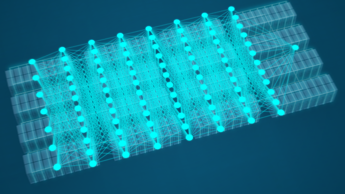
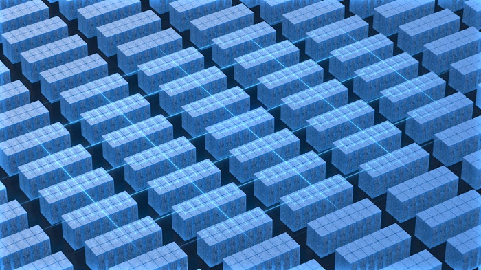
The key with generative AI models is that they are so large that they require global communication across many GPUs — beyond a single chassis or rack in a datacenter. Even for inference (i.e., reasoning and making decisions), the requirements are significant, and even more so for fine-tuning and training. A rough scale looks like this: one rack for inference, tens of racks for fine-tuning, and hundreds of racks for training. Somehow, you’ve got to interconnect all those GPUs.
2. What are the key considerations for interconnecting GPUs?
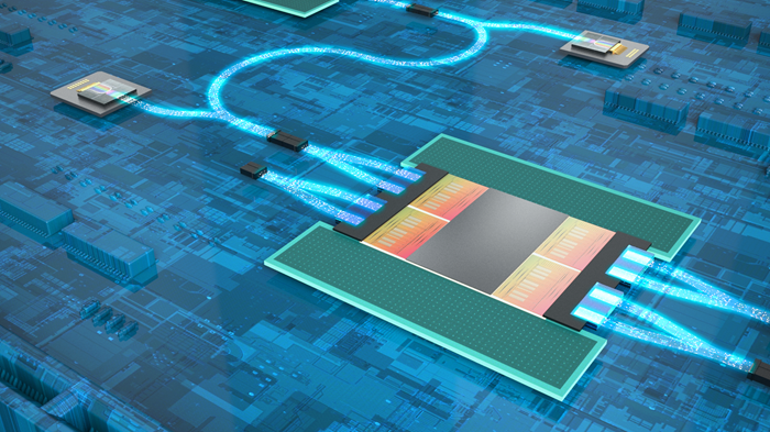
The role of the interconnect in the generative AI architecture above is to provide global communication from every GPU to every other GPU or subsystem, at the full GPU I/O bandwidth and low latency, to maximize the processing efficiency, and with negligible power, area, and cost footprint. Basically, it makes the distributed system look like one giant, virtual GPU. So, the interconnect has got to be extremely fast, dense, and power- and cost-efficient. That’s why Ayar Labs is working to commercialize optical input/output (I/O): it uses silicon photonics to integrate an optical connection at the chip level, producing the fastest and most efficient possible interconnect straight out of the GPU (XPU) package.
3. What is currently being used, and why is it suboptimal?
Currently, these systems rely on pluggable optical connections, which are essentially optical networking technology. Pluggables are great for long-haul applications, like telecommunications, but not designed for on-board input/output.
Pluggables fail for GPU I/O in all four categories: bandwidth/latency, power, density, and cost. Pluggable-based GPU-to-GPU links (or GPU to external switch links) consume ~30 picojoules per bit (pJ/b): 5pJ/b for the initial electrical GPU to optical pluggable link, plus 20pJ/b for the optical pluggable to optical pluggable link, plus another 5pJ/b to convert back from optical pluggable to electrical GPU or switch. Compare this 30pJ/b to in-package optical I/O solutions, which directly connect two packages at less than 5pJ/b — resulting in a nearly 8x power savings.
Pluggables are also bulky modules. Compared to in-package optical I/O, their edge bandwidth density is more than 10x lower and their area density is more than 100x lower than in-package optical I/O. That limits how much bandwidth from the GPU card or chassis can be taken to the rest of the system. Basically, today we’re more or less at the limit and can perhaps squeeze one more generation before the system is completely bottlenecked. Last but not least is the cost. Because pluggables are external modules and not on-board chiplets, their cost scales poorly — for years hovering between $1-$2/Gbps. To enable GPU-GPU bandwidth scaling required for performance scaling of future generative AI systems, this cost needs to be roughly 10x lower. In-package optical I/O can help achieve these cost savings through integration on both the optical chiplet side and the laser side.
4. Can you talk a little about the impact on both training and inferencing? Where do you see optical I/O making the biggest difference?
As mentioned above, there are three applications, each with different footprints and volumes. First, you train an AI model, then you fine-tune it (which can be ongoing), and then you put it into production through inferencing. Given the model scaling trends — from current largest models to the next generation or two, inferencing will take on the order of 10-100 GPUs, fine-tuning 100-1,000 GPUs, and training thousands to tens of thousands of GPUs. Given that a chassis holds at most eight GPUs, and a rack holds 32 GPUs, even inferencing becomes a rack-scale operation where optical I/O is needed.
5. Can you explain the main challenges faced by systems engineers designing for large-scale AI workloads, and how optical I/O addresses these challenges?
First, let’s be clear on who we’re talking about. If we’re referring to machine learning (ML) programmers, then platforms with optical I/O will provide fabric solutions with high throughput scaling, low latency performance, and low latency distribution. Together this allows the entire distributed compute operation to look as much as possible like a single virtual GPU, increasing programmers’ productivity and enabling scalable ML workloads.
If we’re talking about hardware designers who need to build platforms that enable strongly scalable distributed computation, then optical I/O enables physical disaggregation. This is the key to building complex, strongly scalable platforms out of smaller components with a much more aggressive cost-scaling profile. Future designs could conceivably be built around something like a bunch of physically disaggregated GPU compute or switch cards, rather than requiring a complex and expensive multi-GPU chassis.
6. How do you see the role of optical I/O technology evolving in the context of AI model growth and energy consumption over the next five to 10 years?
Optical I/O’s roadmap enables more than a decade of sustained bandwidth and power scaling, which in turn allows for strong distributed compute platform scaling and corresponding model growth.
7. How does “all-to-all connectivity” relate to uniform latency and general efficiency within a generative AI scenario? How can optical I/O help here?
On the extremely large scale required by generative AI (e.g., thousands of compute sockets), all-to-all connectivity has to be achieved through the switching fabric. This must either be distributed across all the compute sockets (such as in TPU-based systems) or separate from compute sockets (such as in GPU-based systems). In either case, optical I/O offers an abundance of bandwidth and low per-link latency at a low power and cost footprint. This allows for a large volume of distance-insensitive optical connections directly out of the compute/switch socket and fabric topologies — what’s known as a fat-tree (or folded Clos) design — that provide short and uniform latency without compromising on the injection bandwidth (the rate at which a node injects data into the network) or bisection bandwidth (the calculation of true overall network bandwidth). Currently, existing fabric designs compromise between fabric cost and performance by using fewer optical pluggable connections — for example, by reducing the bisection bandwidth compared to the injection capacity of compute nodes in fat-tree designs, or by using alternate fabric topologies (such as torus in TPU systems), which minimize the number of rack- and row-scale optical connections, but introduce a nonuniform latency profile, which again limits the application performance.
8. Could you elaborate on the role of optical I/O technology in reconfigurability, particularly in adapting to evolving AI model requirements, and how this flexibility influences system-level efficiency?
In-package optical I/O enables both high bandwidth and a high number of ports (links) out of the compute/switch package, providing flexibility in how the fabric is configured to meet evolving model requirements. For example, the system design could emphasize higher radix (more links), enabling growth in the number of nodes as necessary to support larger model tensor parallelism at lower latencies. Alternatively, it could emphasize higher throughput per link to enable lower transfer latencies with pipelined parallelism.
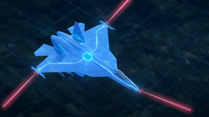
9. Considering the trend toward edge computing for AI applications, what unique challenges and opportunities does optical I/O technology present in delivering high-speed connectivity in resource-constrained edge devices?
Because edge devices have limited resources to work with, physical disaggregation is a key consideration and one of the main advantages offered by optical I/O. For example, aerospace companies are looking to disaggregate next-generation sensors from the underlying compute to rebalance key constraints (e.g., size, weight, and power) while also enabling new sensing configurations that resolve distance (more than one meter) problems (e.g., multi-static radar, synthetic aperture, collaborative MIMO comms, etc.).
10. What are the potential AI performance gains from optical I/O?
We have been creating and evaluating platform developments that — at a chassis, rack, and system level — have the potential to scale-up the fabric throughputs by more than 10x in the next generation. This allows interconnect bandwidth to keep pace with GPU improvements, and AI cluster scale-out trends, ensuring that connectivity is not a constraint for future AI development.
11. As optical I/O matures, what are the key considerations for standardization, interoperability, and ecosystem development to ensure its widespread adoption and compatibility with various generative AI hardware and software frameworks?
Standardization is critical for the overall ecosystem to grow and flourish, and that standardization must have optical I/O as a core consideration. There are two elements here: physical and software.
At the physical layer, there’s the connection itself and the laser that powers the optics. UCIe (Universal Chiplet Interconnect Express)is the standard the industry is coalescing around for a universal interconnect at the package level, combining best-in-class die-to-die interconnect and protocol connections from an interoperable, multi-vendor ecosystem.
For the laser, the CW-WDM MSA (Continuous-Wave Wavelength Division Multiplexing Multi-Source Agreement) is the industry initiative and specification formed to standardize WDM CW sources in O-band for emerging advanced integrated optics applications such as AI, HPC, and high-density optics that are expected to move to eight, 16, and 32 wavelengths.
Both of these initiatives enable a leap in performance, efficiency, cost, and bandwidth scaling compared with other physical layer interconnect technologies.
At the software layer, the future is in protocols such as CXL (Compute Express Link), an open standard for cache-coherent interconnect of processors, memory, and accelerators. This enables such advances as pooled or switched memory, providing the underpinnings for GPUs to leverage the high throughput and low latency of the physical layer to share disaggregated memory.
12. In terms of skillsets and expertise, what are the key qualifications and knowledge areas expected from professionals entering the field of optical I/O development for AI, and how can companies and educational institutions prepare the workforce accordingly?
It is a challenging multi-disciplinary problem — across the stack — from the physics of silicon photonics and lasers to circuit design and computer/network architecture (coupled with manufacturing and packaging), not to mention a system-programming/communication stack for distributed compute/shared-memory systems. Companies, individuals, and educational institutions can best prepare by recognizing and emphasizing this cross-stack design approach.
Thank you, Vladimir, for taking the time to share your insights and perspective on how we can address the architectural challenges companies face in growing and improving the performance of AI models. It should be apparent that optical I/O holds great promise when it comes to enabling the future of generative AI.


Speak Your Mind